Date:2023-10-24
How should we respond to the growing challenges facing our Semiconductor industry?
If we compare transistors to food, we can refer to the solution to the food crisis to illustrate three ways to deal with the challenge of chips.
First, the most immediate is to continue to increase the yield per unit area of staple grains, which corresponds to increasing the density of transistors in chips, known as“More Moore.”.
Second, we should expand other types of grain and increase their richness. This means that in addition to digital chips such as CPU and memory, we should also expand the use of analog, radio frequency, power supply, display and flexible chips, and the ability to integrate functionality through a 3D chip called“More than Moore.”.
Third, and most far-reaching, is the development of entirely new varieties of grain, which corresponds to the exploration of new transistors beyond MOS field-effect transistors, such as carbon nanotube field effect transistors (CNTFET or CNFET) , resistive memory (RRAM) , phase change random-access memory (PCRAM) , tunneling field effect transistors (TFET) , etc. , this path is called Beyond Moore.
01. “Continuing Moore”
The semiconductor industry continues to shrink the size of transistors, increasing the density of transistors on chips, is the“Continuation of the Moore” path the main goal.
When the process nodes went from 5 nanometers to 3 nanometers and 2 nanometers, the FinFET encountered an old problem. The transistor could not be effectively turned off, and the leakage current spiked, causing severe heat. Although FinFET has become a three-dimensional structure that can be turned off by the raised three sides of the channel, but still can not be completely shut off.
In 2003, researchers proposed an even bolder“Nano-wire” structure. In this structure, the transistor's conduct
ive channel becomes a nanosized“Line”, completely surrounded by a ring-shaped“Gate” in all directions, like a“Hand” holding a rubber hose. Applying a voltage to the“Hand” turns off the transistor better, reducing leakage current.
While this structure solves the problem of switching the transistor off, it also has an effect on the amount of current that passes through the transistor when it is turned on: thin nanowire wires are extremely effective at blocking the current.
To this end, in 2006, French Atomic Energy Commission electronic and Information Technology Laboratory (CEA-LETI) researchers proposed Nano-sheet structure. These transistors are called gaafets (see figure 14-3) . In this structure, instead of thin“Wires” connecting the sides of a transistor switch, thin and wide“Sheets” are used, so that the fully enclosed structure is more conducive to turning off the transistor, and multiple thin, wide sheets enhance electrical conductivity. In 2017, IBM showed off the stacked nanochip transistors. In May, the 2021 company IBM a 2-nanometer technology node with a nanochip that incorporates 50 billion transistors on a chip the size of a fingernail.
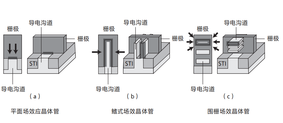
Fig. 14-3 evolution of transistor structure
IRDS predicts that gate transistors will be used in technology nodes of 3 nm, 2 nm and below. Samsung is ready to cut the gate transistor at 3 nanometers, while TSMC is ready to migrate at 2 nanometers.
At subsequent 1-nanometer and 0.7-nanometer technology nodes, the size of individual transistors will once again face challenges. IRDS predicts that the industry will then erect the horizontally positioned gate transistors to further reduce the“Footprint.”. Further, the industry might stack the gate transistors to make a 3D structure. The chips will continue to“Grow” upwards by stacking them up, like layers of gardens in the sky, in order to continue to increase the number of transistors that can be accommodated per unit area.
Even with a good transistor design, it's another matter to make one.
The biggest bottleneck in making transistors remains the lithography machine. The minimum gate spacing that an immersion lithography machine with a light source of 193 nanometers can process is about 34 nanometers. You know, 193 nanometers of UV light (134 nanometers after being refracted by water) can't be used on its own to process such a small size. It needs to be exposed multiple times to separate edges of the lines, to achieve the required precision. However, the smaller the processing size, the more UV light is used for multiple exposures
The number of masking plate will be more, to 7 nanometers technology node will need dozens of mask plate. The more mask, the more processing steps, the more cost and time spent. A 10-nanometer wafer is 32 percent more expensive than a 14-nanometer wafer, and 14 percent more expensive than a 10-nanometer wafer at a 7-nanometer node. If the next generation EUV lithography machine is not used when the 5-nanometer technology node, the lithography steps will reach more than 100 steps.
EUV lithography (see figure 14-4) is the light source wavelength of 13.5 nanometers, only 1/10 of immersion lithography, is the hope to solve this problem. However, the EUV lithography machine has been delayed time after time. As early as 1994, several companies in the semiconductor industry joined forces to launch the industrialization of EUV lithography
Asmail delivered a prototype photoresist scanner in 2006, but then got stuck with a laser source that made EUV light with a wavelength of 13.5 nanometers too difficult to produce.
It wasn't until 2011 that Cymer, a semiconductor equipment company based in Ximeng VA Autonomous County, California, came up with a way to produce extreme ultraviolet lasers. “When I first heard about this idea, I thought it was crazy,” comments Alberto Pirati, a lithography expert at ASMALL, which is to melt metal tin at high temperatures, spray extremely fine droplets evenly into a cavity, then shine a powerful Carbon dioxide laser beam of light at 50,000 strobes per second, and convert it into a plasma similar to that in the sun, which excites 13.5 nanometers of EUV.
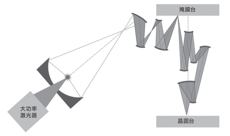
Fig. 14-4 schematic diagram of EUV lithography machine
However, this method is extremely inefficient. The laser requires an input of 20 kilowatts (enough to power 100 refrigerators) , but produces an output of only 11 watts (equivalent to the power of an LED lamp) , far less than the 250 watts needed for lithography, the remaining 99.945 percent of the energy is lost as heat.
Seymour had to find a workaround: a low-power pilot laser would illuminate the droplet particles, “Flattening” them into a pancake shape and increasing the area of light exposure, a high-power laser is then used to excite more EUV light. In 2013, output was increased to 55 watts, and in 2016 to 200 watts. In 2018 it finally reached the 250 watts it needed to actually work.
Although the EUV light source is available, new problems arise. EUV light can not travel through the air because light at such short wavelengths is absorbed by the air. For this purpose, the light path inside the machine and the area where the wafer table is located need to be vacuumed.
To make matters worse, glass lenses also absorb EUV light, forcing people to switch from decades-old lenses to mirrors. However, ordinary mirrors also absorb EUV light. To that end, ASMALL has created a special mirror that is alternately coated with thin layers of silicon and molybdenum, each just a few nanometers thick. Using the Bragg effect of two materials with different refractive coefficients, a portion of EUV light can be reflected at each interface.
EUV light passes through 12 mirrors before reaching the wafer, losing 30 percent of its light each time, and only about 1 percent of its light reaches the wafer. A 250-watt light source hits the wafer, leaving only 2 watts.
Such a weak light needs photoresist extremely sensitive, but high-sensitivity photoresist will cause fluctuations in processing accuracy. ... one technical problem after another, and then another.
After many delays, the company eventually overcame unimaginable difficulties and produced the most sophisticated lithography machine in human history, costing up to $200 million each.
In 2018, asmail began delivering EUV lithography machines to customers. Parts for each machine need to be transported by four Boeing 747 planes. When it arrives at the FAB, there will be hundreds of engineers ready to install and debug it. The lithography machine covers an area of about 80 square meters, of which the laser part occupies 20 square meters. The whole machine is like an iceberg, because a lot of pipes and cables are buried 10 meters below the ground before they come out of the ground.
In 2018, asmail began delivering EUV lithography machines to customers. Parts for each machine need to be transported by four Boeing 747 planes. When it arrives at the FAB, there will be hundreds of engineers ready to install and debug it. The lithography machine covers an area of about 80 square meters, of which the laser part occupies 20 square meters. The whole machine is like an iceberg, because a lot of pipes and cables are buried 10 meters below the ground before they come out of the ground.
In 2020, after 17 years of research and development, EUV lithography machine finally began to be used in the 5-nanometer node manufacturing process. It faces new challenges in the future. Technology nodes up to and including nanometers require higher resolution. At this point, the need for a high“Numerical aperture” EUV lithography machine, and the latter needed to double the power of the light source, to 500 watts.
However, the EUV lithography machine will soon be reaching its limits. The IRDS estimates that, the 2028 half-pitch will reach the limit of 8 nanometers (in addition, although x-rays and electron beams have shorter wavelengths than euvs, they are not considered suitable for large-scale chip manufacturing because they require large, expensive synchrotron radiation sources and the serial writing of electron beams is inefficient) . That would be the“Edge of the cliff”, and beyond that the uncertainty of quantum mechanics rules the world. When the lithography precision reaches the limit, the transistor size will not be able to continue to reduce.
The only way it is possible to continue to increase the density of transistors is to stack multiple layers of chips vertically, which would be like turning a single-story house into a high-rise building to increase the density of transistors. In fact, prior to EUV lithography, 3D stacking was already being used to make cost-sensitive memories, allowing cost control without the need for state-of-the-art lithography. At present, memory has been implemented hundreds of layers of stacking.
In addition to the above difficulties, the CPU performance improvement is getting slower and slower. In the 1990s, CPU performance increased by 52% a year. In the 2000s, it increased by only 23% a year. From 2011 to 2015, it fell by nearly half, to 12.5% , between 2015 and 2018 it was almost flat at 3.5% .
Moreover, the"Memory wall" between CPU and memory is becoming increasingly difficult to cross. The von Neumann computer first pulls data from memory and feeds it into the CPU for calculation. However, the CPU processing capacity significantly improved, the speed of the computer to fetch data from memory did not increase proportionally, so the formation of a bottleneck between the CPU and memory channel.
The CPU quickly"Digest" the data in the"Belly", but the new data can not be"Fed" from memory, the CPU has to be in a"Hungry" state. It is estimated that the time it takes a computer to move data from memory is at least 10 times longer than the CPU, which wastes precious time and resources waiting.
There are many reasons for the"High wall" between CPU and memory, one of them is the distance between CPU and memory, they are located in different chips, easy to cause signal delay. To shorten this distance, it is proposed to package CPU and memory in the same chip, put them in different layers, and then stack them into a three-dimensional chip, layer by layer connected by silicon through-hole, to shorten the signal transmission distance. However, even though the CPU and memory are in different parts of the same chip, the delay on the interconnect is getting worse.
The way to completely solve the"Memory wall" problem is to change the way the CPU fetches data from memory, instead of centering on the computing unit, it focuses on the storage instead, the development of computing, storage integration of"Memory computing.". The new architecture has the potential to change the dominance of the "80-year-old" von Neumann computer architecture.
02. “Extend Moore”
As the barriers to continuing Moore grew, people began to look for other solutions. In 2005, ITRS came up with the concept of“Extended mole”. This path seeks not to reduce the size of a single transistor, but to increase the diversity of the system's capabilities, integrating and implementing a wealth of capabilities on a single chip.
This path focuses not on the most advanced digital chips, such as cpus and memory, but on analog, power, sensing, and mixed-signal chips, which do not require the smallest transistors, but can realize the rich application scenario.
“Scale Moore” drives technology development based on top-level applications and needs, one of the biggest needs being the Internet of things. Personal computers and mobile phones have become ubiquitous in the past few decades, but they are reaching saturation point and will increase by up to three times in the future. The future of iot devices, including smart homes, health monitoring, self-driving cars and Environmental monitoring, will add another three orders of magnitude to a ubiquitous iot world.
For example, self-driving cars need a variety of sensors such as laser range finders, ultrasonic sensors and accelerometers, and medical fields need wearable physiological-signal monitoring equipment, implanted sensors and current-stimulation chips are needed to suppress seizures, and the Environmental monitoring sector needs chips that can detect a variety of pollutants such as carbon dioxide and sulphides. These sensors need to be integrated with the CPU, memory, and so on, to achieve rich functionality.
In addition, we also need efficient power supply, want to achieve extremely low power consumption, to meet the requirements of portable or mobile devices. Takanobu sensors and analog circuits are also needed to sense or capture weak physiological signals, concentrations of dangerous gases, and so on. We also need to meet a wide range of radio frequency circuits, to achieve more diverse wireless connectivity.
Another area where there is an“Extended mole” need is in the energy sector. Gallium nitride and silicon carbide are superior to silicon in List of semiconductor materials performance and can be used to make power devices that provide higher switching frequencies at the same withstand voltages, or lower on-off and switching losses at the same withstand voltage and switching frequency.
In addition, there will be a great demand for energy-harvesting technologies, as many of the sensors are located in open-air environments where there is no mains power supply and it is not easy to replace the batteries. Energy can be collected through mechanical vibrations, differences in temperature between hot and cold, or radio waves, light, and so on, which will greatly extend the working time of the chip.
Finally, flexible electronics will play a role in fabric-based wearables, folding screens, and thin-film solar cells. In the future, a large part of flexible electronic devices will be made by printing on flexible substrates, but the industry needs to make further breakthroughs in organic and carbon-based materials.
Starting in 2017, a technology called Chiplet attracted interest from the industry, especially Advanced Micro Devices companies. In the past, people try to integrate different circuit modules into one chip to reduce the cost. But it has been found that the larger the area of the chip being processed, the lower the yield (the proportion of good, bare chips on a wafer) , pushing up costs. On the contrary, the big chip into small chip can improve yield, reduce costs.
Thus, a reverse trend has emerged: large chips are broken down into smaller individual chips, manufactured separately, and then combined together by packaging (see figure 14-5) . It's a bit like making small Lego blocks and then putting them together into a larger whole. For example, a chip with an area of 360 square millimeters can be divided into four small chips, and its yield will increase by more than three times. In this trend, there will be more and more cores in future cpus. A Advanced Micro Devices company's “Dragon” processor, or EPYC, has eight small chips, each with eight more cores, for a total of 64.
The small chip technology adds a degree of freedom to the chip system, that is, each small chip can freely use the best cost-effective technology, CPU and memory use advanced technology to improve computing power, and the simulation and radio frequency are more low-cost mature technology to reduce the overall cost.
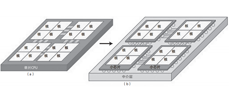
Figure 14-5 splits a single chip (a) into small chips (b) and connects them through the substrate below
When Keelby and Neuss invented the integrated circuit in 1958 and 1959, they solved the problems of integration and interconnection respectively. Now more than 60 years later, we are still on the road to finding ways to better integrate and interconnect. The way of integration is from plane to three-dimensional, from single chip to multi-chip, from single circuit interconnection to digital, analog, RF, sensor and so on, from silicon integration to silicon, carbon, germanium and other elements of the common integration, from the plane to the three-dimensional interconnection.
03.“Beyond Moore”
The computing demands of new technologies such as big data, the Internet of things, artificial intelligence and supercomputing are putting higher demands on chip performance and energy efficiency, so there is a third way: “Beyond Moore”, also known as“Beyond CMOS,” that is, outside the mainstream CMOS technology to find a better possibility.
Leakage current in silicon transistors has long been a worry for scientists. To this end, TFET was invented (see figure 14-6 for its structure) . It uses the quantum tunneling effect between the conduction band and the valence band to control the transistor's on and off, making the leakage current smaller and the conduction current larger, breaking through the Maxwell–Boltzmann statistics limit in the traditional transistor, the sub-threshold swing is lower than the lower limit of 60 mV/DEC.. However, the source and drain of TFET are no longer P-type semiconductors or N-type semiconductors like MOS field effect transistors, but P-type semiconductors on one side and N-type semiconductors on the other, this presents a new challenge to device manufacturing and application.
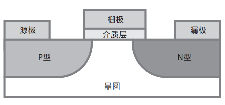
Figure 14-6 structure of the TFET
Although silicon is suitable for large-scale production, is abundant in storage and has a naturally stable insulating oxide layer, it also has insurmountable disadvantages, such as low Electron mobility, resulting in low switching speed, and general heat dissipation, limits the chip's operating frequency. All these problems make it difficult to“Continue Moore”.
Carbon materials, on the other hand, have advantages in mobility, small size and heat dissipation. In the lab, researchers have made CNTFET (see figure 14-7) from carbon nanotubes, a structure similar to silicon MOS field-effect transistors, just replace the conductive channel in the middle with carbon nanotubes with better mobility, better heat dissipation and smaller size. The challenges of large-scale preparation are still being addressed.
 Fig. 14-7 CNTFET NOTE: Top View (a) and side view (b)
Both BJT and MOSFET devices use electrons as the medium of information processing, and the innovative idea is to use faster photons. The photon has no heat dissipation problem, is not affected by the electronic noise, and the optical signal delay is small, the communication bandwidth is much higher than the electrical signal.
In addition, all kinds of optical processing devices (optical waveguides, optical filters and optical connectors) can be made from silicon, which can be easily integrated into CMOS chips, thus greatly reducing the cost. Making Optical Interconnect processors is starting to become possible. However, silicon optoelectronics still need to break through some technical bottlenecks to enter the practical application.
In 1970, professor Leon Leon O. Chua of the University of California, Berkeley, discovered that there were already three basic components: a resistor, which correlated voltage and current, a capacitor, which correlated voltage and charge, and an inductor, which correlated voltage and current, responsible for the correlation between current and magnetic flux. But can charge and magnetic flux be directly related? Leon O. Chua suggested that there might be a fourth basic element that could directly relate charge to magnetic flux, which he named memristor (see figure 14-8) . In 2008, a team led by Wilhemlms of Hewlett-packard laboratories made memristors with a single-device structure, consisting of only metals at the ends and oxides in the middle.
Memristors have a resistance-memory effect, which maintains a resistance value after a power failure and changes it when stimulated by a pulse, just as synapses in the brain change the strength of connections when stimulated by a neuron pulse, it can be used as an artificial electronic synapse to simulate the chemical synapse in the brain and realize the function of learning and memory. The size of memristor can reach nanometer level, but there is still much room for improvement in yield and device consistency.
In addition, spin-field-effect transistors (Spin-FET) , PCRAM, RRAM, magnetoresistive random-access memory (MRAM) and flexible thin film transistors (FTFT) have also been studied, however, due to the low cost and large output of traditional devices, the advantages of these new devices can not be reflected, can not replace the existing devices in the short term.
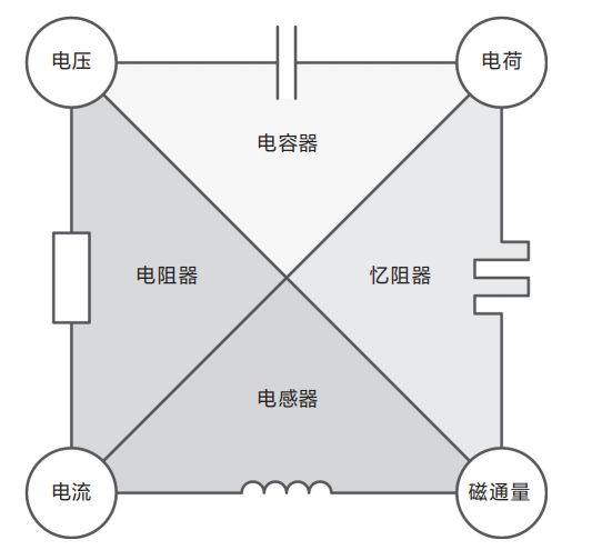 14-8 the relationship between the four basic components
Note: The diagram shows the correlation between the three basic elements (resistors, capacitors, and inductors) and the fourth basic element -- memristors -- as envisioned by Leon O. Chua.
However, “Danger” hidden“Machine”. The end of the transistor-shrinking path may be good news, since most of the industry's money and manpower has been spent on research related to silicon MOS MOSFET devices, to maintain the speed predicted by Moore's law. Now, the end of Mos Fet size reduction will make way for the development of non-MOS FET devices.
In the field of EDA chip design, with the integration of digital, analog and RF circuits into one system, the electromagnetic interference will become more complex, and the problem of heat dissipation and performance degradation need to be handled more carefully, interfaces between different circuits also become more complex. In recent years, artificial intelligence has been used to solve the problem of chip wiring in order to find the optimal solution.
At the application level, in order to meet the computing needs of different scenarios, high Bandwidth Memory (HBM) , in-memory computing, near-memory computing, neuromorphic computing, approximate computing and chip technology integrating sense memory are being studied.
Will all these ideas come true in the future? We don't know for sure, but they are sure to come along in ways we've never seen, heard, or even imagined, and shatter claims we once believed in. To paraphrase the computer scientist Ellen Kay, “The best way to predict the future is to invent it.”
: : Disclaimer: all original and republished statements and opinions are neutral, and articles are only sent for readers to learn and share. Articles, pictures and other copyright to the original author to enjoy, if there is infringement, contact delete. This article is reprinted from (core event public)