Advantages of flat wire process inductors: Flat wire process inductors have significant advantages in practical applications, including the following points:
1. * * Higher Energy Efficiency * *: The magnetic core inside the flat wire process inductor is designed as a surround, which can minimize the loss of the magnetic core and make the transmission of electrical energy more efficient, thereby reducing the energy consumption of the system.
2. * * Better Electromagnetic compatibility * *: The internal structure of the flat wire process inductance is compact, which makes the electromagnetic interference of the inductance less and has less impact on other electronic equipment, thus improving the Electromagnetic compatibility of the system.
3. * * Longer service life * *: Due to the tighter magnetic core inside the flat wire process inductor, the loss of the magnetic core is smaller, thereby extending the service life of the inductor and reducing the frequency of replacing the inductor.
4. * * Smaller Volume * *: The design of the flat wire process inductor makes it smaller and easier to install in narrow spaces, which is of great significance for the design of portable and miniaturized devices.
5. * * Better heat dissipation performance * *: The winding inside the flat wire process inductor adopts a flattened design, with smaller gaps between the windings, which helps to improve the heat dissipation performance of the inductor and reduce the failure rate caused by overheating.
6. * * Easy to customize * *: The design of flat wire process inductors is flexible, and inductors of different sizes, currents, and magnetic core materials can be customized according to different application needs to meet the diverse needs of users. By customizing the design, the performance of the inductor can be further improved to meet more stringent electronic system requirements. In a word, the flat wire process inductance has many advantages and is widely used in the electronic industry, especially in the fields of high efficiency, high Electromagnetic compatibility, long life and portable equipment.
In practical applications, the advantages of flat wire process inductors have also been widely recognized. For example, in new energy vehicles, the use of flat wire process inductors can reduce the energy loss of the entire vehicle, thereby increasing the range of new energy vehicles. In the field of smart homes, flat wire process inductors can make household energy consumption more efficient, reduce household energy costs, and also be beneficial for environmental protection. In addition, in fields such as communication base stations and 5G networks, flat wire process inductors also play an irreplaceable role.
In summary, the advantages of flat wire process inductors are obvious, and their application prospects in the electronics industry are very broad, with great development potential. With the continuous progress of technology, the performance and application range of flat wire process inductors will also be further expanded, providing strong support for the development of the electronics industry.
When designing a circuit, methods to pay attention to when applying inductance:
1. Determine circuit requirements: Before designing a circuit, it is necessary to first clarify the requirements of the circuit, including its functions, performance indicators, working conditions, etc., in order to select appropriate circuit parameters and devices.
2. Select appropriate devices: Select appropriate devices based on circuit requirements, including resistors, capacitors, inductors, diodes, transistors, etc., and design component values reasonably to ensure circuit performance.
3. Choose a suitable topology: Select the appropriate topology structure according to the circuit requirements, such as star, triangle, tree, ring, etc., to improve the stability and reliability of the circuit.
4. Analyze circuit parameters: Analyze the circuit to determine circuit parameters, such as inductance value, power supply voltage, current, etc., to ensure the rationality of circuit parameters.
5. Conduct simulation verification: Simulate the circuit to verify whether the performance indicators of the circuit meet the requirements, adjust the circuit parameters in a timely manner, and ensure that the circuit performance meets the requirements.
6. Compile Software design description: sort out and summarize the information related to circuit design, and compile Software design description, including circuit schematic diagram, PCB layout, device list, etc., to provide basis for subsequent production and testing.
7. Making PCB board: make PCB board according to the Software design description, and weld and debug the components on the board to ensure the normal operation of the circuit.
8. Conduct testing and debugging: Test and debug the completed circuit, including power supply testing, performance testing, environmental testing, etc., to ensure the stability and reliability of circuit performance.
In short, the following Committed step should be taken when designing the circuit:
1. Requirement analysis: Communicate with the project leader, clarify project objectives, understand project requirements, and develop detailed design plans.
2. Device selection: Based on the analysis results of the requirements, select suitable devices, including resistors, capacitors, inductors, diodes, transistors, etc., to ensure that the device performance meets the requirements.
3. Determine topology structure: Based on project requirements and device selection, select appropriate topology structures such as stars, triangles, trees, rings, etc. to ensure circuit stability and reliability.
4. Circuit parameter analysis: Analyze circuit parameters to ensure that they are reasonable and meet performance requirements.
5. Conduct simulation verification: Simulate the circuit to verify whether the circuit performance indicators meet the requirements, adjust the circuit parameters in a timely manner, and ensure that the circuit performance meets the requirements.
6. Compile Software design description: sort out relevant information of circuit design, and compile Software design description, including circuit schematic diagram, PCB layout, device list, etc., to provide basis for subsequent production and testing.
7. Making PCB board: make PCB board according to the Software design description, and weld and debug the components on the board to ensure that the circuit works normally.
8. Testing and debugging: Test and debug the completed circuit to ensure stable and reliable circuit performance.
Through the above design process, circuit design can be better planned and managed, improving circuit performance and quality, and providing strong support for the research and production of the final product. At the same time, reasonably arranging time and focusing on Committed step will help improve circuit design efficiency and reduce project risks. In short, circuit design requires a meticulous work attitude and solid professional knowledge, and efficient process management and reasonable time planning are key factors for success.
1. Filtering and anti-interference
As an energy storage component, an inductor can suppress high-frequency interference in the circuit and also prevent the influence of low-frequency noise, playing a filtering role. Its magnetic flux can effectively constrain high-frequency signals, prevent their propagation in the circuit, and thus achieve attenuation and filtering of high-frequency noise.
2. The role of inductance in power adapter
In the power adapter, inductance can suppress electromagnetic interference and improve the stability and reliability of the power adapter. When the current passes through the inductor, a reverse magnetic field is generated, which cancels out the forward magnetic field generated by the current, thereby achieving stable voltage output.
3. The role of inductance in filters
The role of inductance in filters is to separate noisy signals from useful signals. Here, the inductor acts as a low-frequency cutoff and a high-frequency cutoff. A low-frequency cutoff can block signals below a specific frequency, while a high-frequency cutoff can block signals above a specific frequency. Through such a combination, the filter can effectively isolate noisy signals from useful signals.
4. The role of inductance in transformers
Inductance mainly plays the role of a magnetic core in a transformer, converting the input AC power into the output AC power. Transformers can achieve voltage changes by utilizing the magnetic energy storage and release of inductors, thereby completing the transmission and distribution of electrical energy.
5. The role of inductance in the Electronic oscillation circuit
In the Electronic oscillation circuit, the inductance can act as an energy storage element, so that energy can be quickly released when needed. When an external voltage is applied to the inductor, it will generate self induced electromotive force, which is opposite to the direction of the external voltage. This phenomenon is called electromagnetic coupling, which prevents the current in the inductance from immediately changing. This delay phenomenon allows the inductor to act as a frequency selective component, selectively passing through signals of a specific frequency. This frequency selective characteristic is very important in the Electronic oscillation circuit, because only under the action of a specific frequency signal, the oscillation circuit can produce stable oscillation signals. In this process, inductance plays an important selective role, causing the oscillation circuit to only respond to signals of a specific frequency.
The role of magnetic beads in circuits: Magnetic beads are a specially designed inductor with high permeability and resistivity. Its working principle is different from traditional inductors, but is based on its high permeability and low resistivity characteristics to solve electromagnetic interference problems in circuits. The main functions of magnetic beads in circuits are as follows:
1. Suppression of electromagnetic interference: Magnetic beads can absorb and reduce high-frequency alternating electromagnetic fields passing through the circuit. This is because the magnetic domains in the magnetic bead can interact with the electromagnetic field, generating eddy currents, thereby offsetting the effect of the electromagnetic field. This can effectively eliminate electromagnetic interference and ensure the stable operation of the circuit.
2. Protection of sensitive circuits: Magnetic beads can also prevent damage to sensitive circuits caused by high voltage and high current in the circuit. Due to the high resistivity of magnetic beads, the heating of magnetic beads under high voltage and current conditions will not cause damage to the circuit.
3. Reducing electromagnetic radiation: Magnetic beads can also effectively reduce electromagnetic radiation. Because magnetic beads can absorb energy from electromagnetic fields, thereby reducing the intensity of electromagnetic radiation.
4. Improving circuit performance: Magnetic beads can also improve circuit performance. Because magnetic beads can absorb energy from electromagnetic fields, thereby reducing electromagnetic interference in the circuit and improving its stability and reliability. At the same time, the high permeability of magnetic beads can also increase the signal transmission ability of the circuit and improve its performance.
In summary, the role of magnetic beads in circuits is very important. They can effectively eliminate electromagnetic interference, protect sensitive circuits, reduce electromagnetic radiation, improve circuit performance, and ensure stable operation and high performance of the circuit. In addition, magnetic beads have the advantages of small size, light weight, high reliability, and easy installation, making them widely used in various electronic devices and systems. For example, magnetic beads play an irreplaceable role in fields such as communication systems, computer systems, automotive electronics, and medical equipment. In short, the role of magnetic beads in circuits cannot be ignored and is an important component of ensuring the stable operation and high performance of electronic devices and systems.
1 磁组合电感的定义
由不同的磁性材料,一个或多个电感组合设计在一起的电感要素 :
1不同的磁性材料组合在一起,
2一个或多个电感组合在一起。
观点:有部分工程师命名为磁集成电感,实际上集成和组合的区别是,集成是电子中多个器件集成封装在一起,是不可物理分割的(比如,集成电路是由电阻 R、电容 C、二极管D、三极管O等集成封装而成).而磁组
合是可以物理分割的
2磁芯材料重要参数
电感所用磁芯常用几大类 :
1:软磁锌铁氧体类(Mn-Zn Ferrite Core)
2:铁硅铝(KooL Mu或 Sendust)
3:铁合金(Fe-Si)
4:高磁通粉(Hi-Flux)
5:铁镍磁粉芯(Mpp Core )
6:硅钢片(Si-Steel)
2.1、 软磁锌铁氧体类(Mn-Zn Ferrite Core)
按照预定的配方称重,把高纯、粉状的氧化物( 如Fe,O;、Mn,O,Zno等)混合均,再经过预烧、粉碎、造粒模压成型为毛坯,在高温(1200C ~1400C)下烧结,再通过磨削加工而成
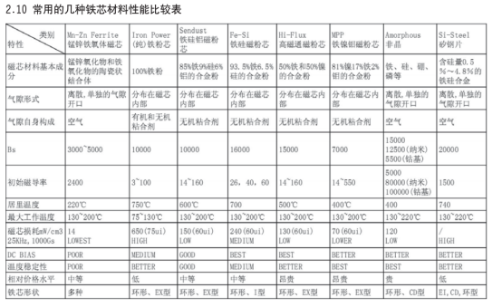
锰锌铁氧体具有最低的铁芯损耗、价格低廉、可加工性强、可选磁导率多(1400~18000),缺点是 B相对较低易碎;广泛应用于开关电源变压器、扼流圈、EMI 滤波器通讯领域宽带、脉冲变压器等。
锰锌常用规格:EE、EF、EI、ER、ET、UT、UU、T、RM、EP、POT、EPC、EFD、UI 等等.
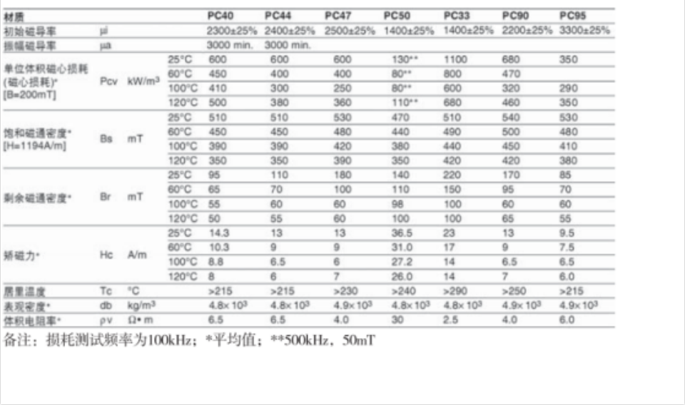
电感用锰锌铁氧体一般选用功率型系列材质:PC40PC44、PC50、PC47、PC90、PC95 等

2.1.1以长江微电为代表的常用材质基本参数
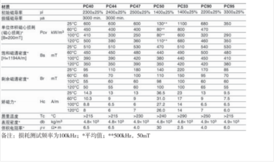
2.1.2 不同材质锰锌铁芯损耗--- 温度对比曲线图
(以长江微电材质为代表)
PC40:价格优,适用要求不高的场合
PC44:在高温时比PC40 损耗低
PC95:宽温低损耗,待机损耗低
PC47:高温低损耗,价格贵
PC90:高 BS,常用于储能电感
2.1.3不同材质锰锌铁芯损耗--- 频率对比曲线图(以长江微电材质为代表 )

2.2、铁硅铝 Sendust Core
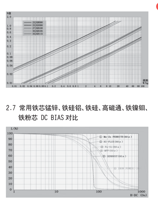
铁硅铝由铝 6%,硅 9%,铁 85% 组合成,磁导率在14~173 之间。损耗和成本比铁硅合金低。铁硅有非常低的磁滞伸缩系数,特别适合于要求低音频噪声的场合
铁硅铝在交流激励下的电感量变化最小,在高温下具有极佳的温度稳定性,同时,随着温度的升高,电感量下降,而其它的材料却是随着温度的升高,电感量增加。因此对于需要温度补偿的场合可以采用铁硅铝和其它材料的复合结构
2.2.1 铁硅铝典型 DC BIAS 曲线

2.2.2铁硅铝损耗曲线
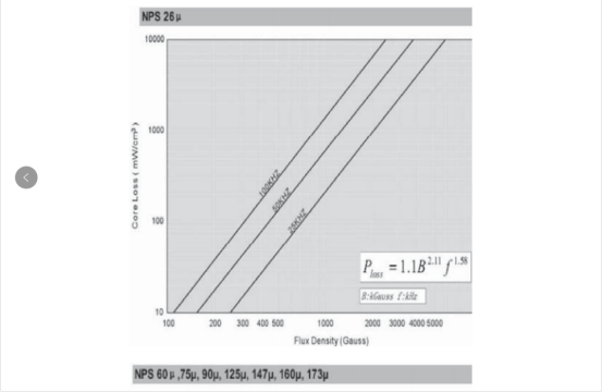
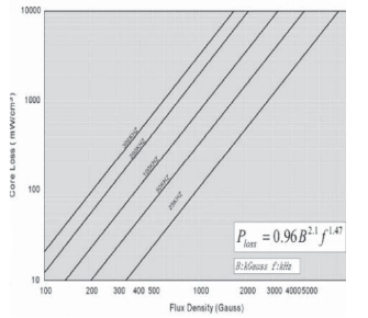
2.3、铁硅合金(Fe-Si)
铁硅由 Fe 93.5%,Si 6.5% 组合成,常用导磁率有26ui、40ui、60ui、75ui、90ui 等
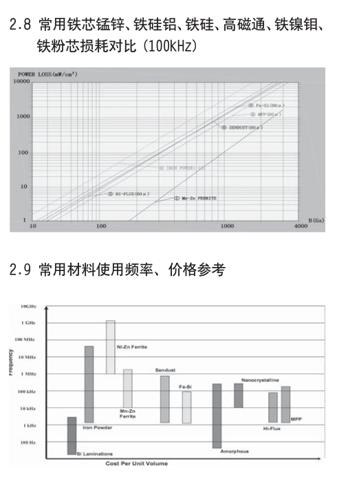
铁芯损耗介于铁粉芯与铁硅铝之间,具有很高的储存能力和高的 B(16000Gs)。DC BIAS 能力和 Hi-Flux 相当但损耗比其要大,在价格上有很大的优势铁硅合金常用于大功率 PFC、储能电感、逆变电感等

2.3.1 铁硅典型 DC BIAS 曲线

2.3.2 铁硅损耗曲线
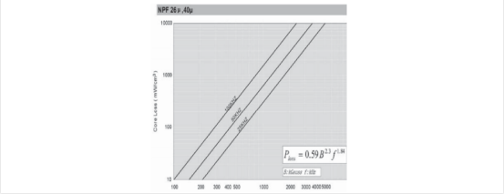
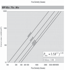
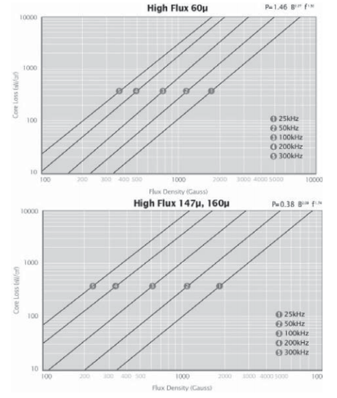
2.4高磁通磁粉芯(Hi-F1ux)
由铁镍各 50% 组合成,磁率在 26~147ui。高磁通有高的储存能力和高的 B(15000Gs)。高磁通磁粉芯比铁硅合金损耗更低,但比 MPP CORE 损耗稍高,具有优异的 DCBIAS 能力。
它是开关电源调制器、线路噪音滤波器、脉冲变压器和回扫变压器磁芯的理想选择。特别是在大直流电流场合下,使用高磁通磁粉芯可以有效减小电感尺寸 ;
该材料的剩余磁感强度几乎为 0,是脉冲变压器和反激式变压器的理想材料。由于可选规格不多,且价格昂贵它不如MPP、Sendust 和 Fe-Si常用。
2.4.1高磁通磁粉芯典型 DC BIAS 曲线
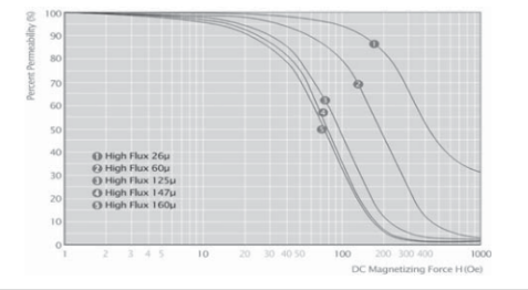
2.4.2高磁通磁粉芯损耗曲线
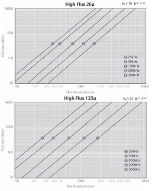
2.5 铁镍磁粉芯(MPP Core)
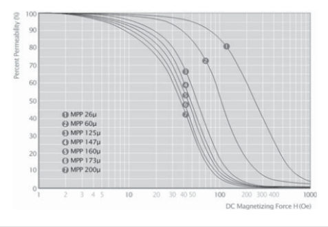
由 81% 镍,17% 铁,和2% 组合成,磁导率在 14~250之间
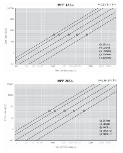
在所有磁粉芯中,MPP 具有最小的磁芯损耗和最好的温度稳定性。
MPP 磁芯具有高电阻系数、低磁滞低涡流损耗,在高DC 磁化或 DC 偏置条件下,电感稳定,具有最宽的磁导率可选范围,是开关电源中直流输出滤波器最佳选择材料。
2.5.1 铁镍磁粉芯典型 DC BIAS 曲线
2.5.2铁镍磁粉芯损耗曲线

2.6 硅钢片(Si-Stee1)
2.6.1 硅钢片分类
热轧硅钢片 :将 Fe-Si合金用平炉或电炉熔融,进行反复热轧成薄板,最后 800-850C退火后制成。热轧硅钢片可利用率低,损耗大,目前已经基本淘汰。
冷轧无取向硅钢片:其含硅量 0.5%-3.0%,经冷轧成不同厚度,(多为 0.2mm~0.5mm)的钢带。冷轧无取向硅钢的 Bs 略高于取向硅钢;与热硅钢相比,其厚度均匀尺寸精度高,表面光滑平整,从而提高了填充系数和材料的磁性能
冷轧取向硅钢片 :与冷轧无取向硅钢相比,取向硅钢的磁性具有强烈的方向性 ;在易磁化的轧制方向上具有优越的高磁导率与低损耗特性。取向钢带在轧制方向的铁损仅为横向的 1/3,磁导率之比为 6:1,其铁损约为热轧带的 1/2,磁导率为后者的 2.5 倍
冷轧硅钢片又分白片( 无烧) 和黑片(有烧,改善结品,降低损耗,恢复磁导率 )
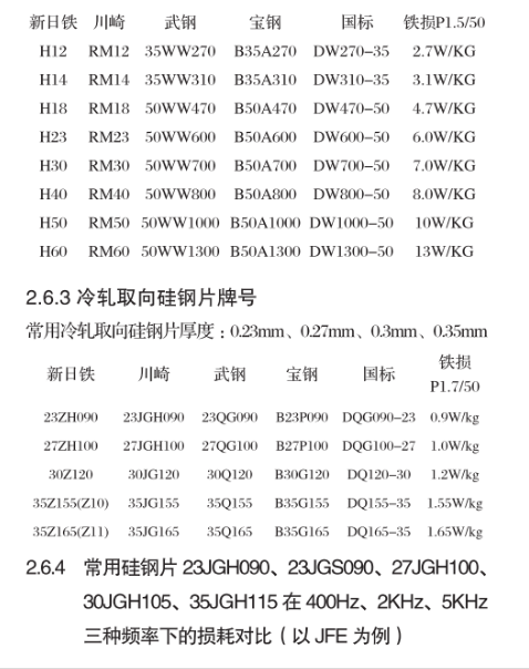
2.6.2冷轧无取向硅钢片牌号
常用冷轧无取向硅钢片厚度:0.35mm、0.5mm
3磁芯的几种组合方法及设计注意事项
3.1 硅钢片和铁硅组合
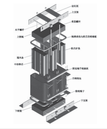
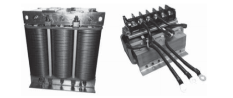
此搭配方式多用于大功率三相电抗器,使用硅钢片做铁扼,更容易获得比较平衡的电感。随着技术的进步,大功率设备使用频率越来越高,传统设计的电抗器一般使用频率为 3kHz 左右,而采用此种磁组合方式可以使产品应用频率达到 5-10kHz,大大减小了产品的体积和成本。
3.2 硅钢片和铁硅组合
注意事项 :
1:铁扼和铁柱之间加0.5mm 左右气隙
2:设计磁通密度一般不超过0.8T
3:频率比较高时,尽量采用高频特性好的JGH 系列硅钢片,频率低时一般采用JGS 系列硅钢片,硅钢片厚度一般选用0.3mm以下
4:导体电流密度,铜一般取 2.5A/mm’以下,铝一般取1.4A/mm以下
实际案例图片 :
3.3铁氧体和铁硅铝、铁硅等搭配
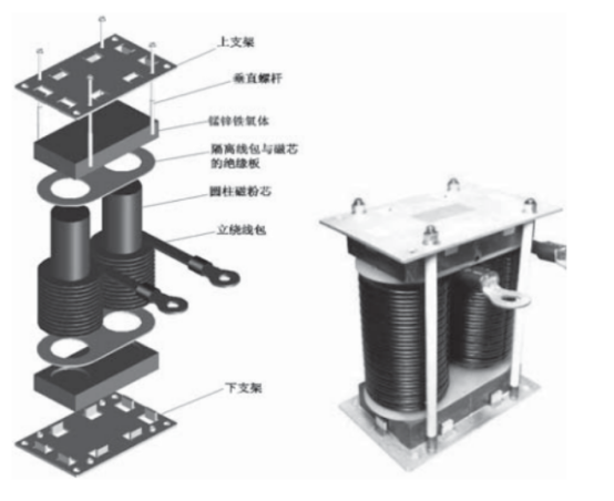
注意事项 :
1:铁氧体一般使用高温下高 B值,高温下DC BIAS特性优良的材质
2:铁柱采用铁硅铝或铁硅,铁采用锌铁氧体
3:锌铁体截面积一般比铁硅铝或铁硅大 20%
3.4 铁硅铝和铁硅磁粉芯搭配
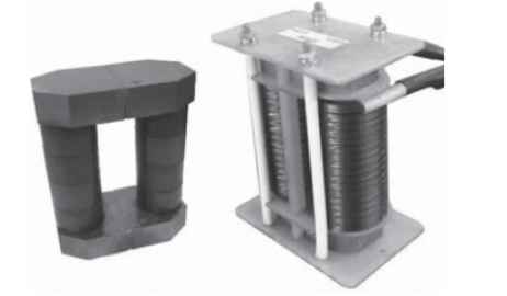
由于铁硅铝B达到 10000Gs,比铁氧体高很多,损耗只有铁硅的 60%,和铁硅组合后具有不错的 DC BIAS 和相对较低的损耗,用于中、大功率电感中具有较好的效率和成本。
注意事项
1:铁一般使用铁材料
2:铁硅铝截面积比铁硅略大
3: 尽量减小铁柱之间的气隙,采用低 ui 值材料
4:线圈尽量使用连绕工艺
磁组合设计的八大优点
优点 1.提升效率
目前,所有用户对用电设备的效率越来越重视,尤其大功率电力电子设备方面,如光伏发电逆变器最高效率要求达到 99% 以上,电感设计思路、方法必须创新,磁组合电感正是基于此理念的新型设计
最近几年,基础材料有较大的进步,研发出多种新的磁性材料,电感的设计有一个台阶式的进步,电感的设计不再是由单一的一种材料组成,为了提升效率,发挥各种材料的优异性能,采用多种材料组合在一起设计,从而提升整机设备效率
优点 2.降低成本
高性价比始终是客户的追求。为满足客户高性能的要求,若采用某一种价格便宜的材料设计可能难于满足客户性能的要求,而采用高性能的材料设计则价格昂贵 ;
因此,采用多种材料(如:硅钢片、超级铁芯、铁氧体非晶、铁硅铝、铁硅等)的合理搭配,发挥各种材料的优点得以满足客户性能要求同时大大降低成本
同时,也可采用一个或多个电感组合在一起,通过局部磁路共用减少材料的使用,从而降低成本。
优点3.降低温升
传统设计 :
传统电感设计使用了大量的绝缘材料,使产品的散热性能差,导!瓜致温升高。
特别是大功率电感采用箔绕的方式,在磁场和电流邻近效应的影响下,产品涡流损耗很大,难于克服。
磁组合设计 :
采用立绕设计,大大减少了绝缘材料的使用,提升了散热性能。
减少了绕线层数,降低了磁场和电流邻近效应的影响大大降低了产品温升。
优点4.减小体积
基于铁芯的合理搭配,有效的发挥各种铁芯的特性提高了铁芯的使用磁通密度范围磁路的共用使电感体积大大减小。
磁组合电感的设计大大提高了应用开关频率,也是减小电感体积的关键所在。
优点 5.降低噪音
传统电感设计采用硅钢片、超级铁芯、非晶、铁氧体时需要额外增加很大的气隙,漏磁和损耗很大,噪音难于避免新设计采用新型材料如铁硅铝、铁硅等均匀气隙的铁避免了漏磁的产生,改善噪音。
新型电感采用不同材料组合设计,使用铁芯分段组合大大减小了漏磁,有效地降低了噪音
优点 6.适应模块化、高频化发展趋势
光伏发电逆变器的设计,为了降低设计成本,未来大功率逆变器逐渐实行组串式模块化设计,基于磁组合电感设计的优点,使用频率从传统电感的 3kHz 提高到几十kHz,未来可能提高到上百 kHz。
优点 7.改善 EMI、EMC 适应
传统电抗器采用箔绕,层数较多,散热效果差,产品分布电容大,邻近效应严重.
磁组合电抗器采用扁线立绕方式绕线,绕组只有一层.大大降低了产品的分布电容,减小了邻近效应、减小电感漏磁,降低了温升,从而使产品获得了优异的 EMI、EMC 效果优点
优点 8.提升产品品质可靠性
磁组合电感结构简单利于操作、生产,安装简洁绕线采用专业设备,可一次完成,无需额外连接整个设计思路达到零故障设计,从而具备极高的可靠性。